Semiconductor production is a field where accuracy and cleanliness are paramount. Every operation and every task is designed to attain the highest levels of precision. Here, the process of plasma descum is a cornerstone.
This specialized technique is crucial for the thorough cleaning of semiconductor wafers, ensuring that no trace of photoresist remains after the development phase. Though these leftover layers are incredibly thin, they can introduce significant obstacles to the nuanced steps of patterning and etching that are fundamental to crafting semiconductors.
In this piece, we dive deep into the world of plasma descum, exploring its procedures, applications in technology, and its contribution to bolstering the quality and performance of semiconductor units.
What is Plasma Descum?
Plasma descum is a cleaning step in the process of making electronics like computer chips. After designing a pattern on a semiconductor wafer with a light-sensitive material called photoresist, there can be thin, leftover layers of this material that need to be removed.
Photoresist descum is like cleaning up leftover bits of a special material called photoresist, which are left behind in tiny trenches or holes on a semiconductor wafer after certain steps in the manufacturing process.
Why is Plasma Descum Important?
Even though these leftover layers are incredibly thin, they can cause problems, especially when the patterns on the chips are remarkably tiny and intricate. If they aren't removed, the next step, etching the pattern into the semiconductor, might not be precise, leading to issues with the chip's performance.
These little leftover bits are tiny, on the scale of nanometers, billionths of a meter, but even at that size, they can cause problems. If they aren't cleaned up, they can mess with the evenness of the next steps of etching or adding metal layers.
How Does Plasma Descum Work?
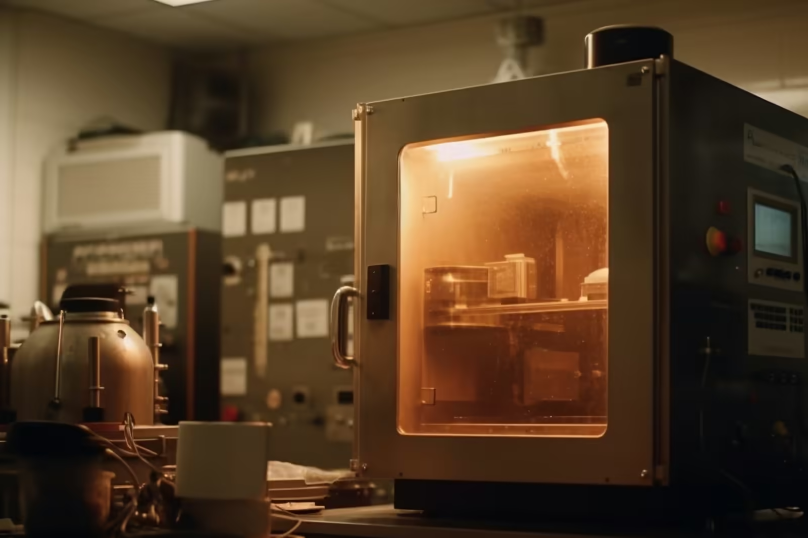
The wafers, with the unwanted thin layer of photoresist, are placed in a special chamber. In this chamber, a plasma (an ionized gas) made of oxygen is used to clean off these layers. This process can be done quicklybut it must be controlled carefully to avoid damaging the underlying pattern or photoresist layer.
This cleanup, or descum, is often done using oxygen plasma, which is like a special type of gas that's been energized to help with the cleanup. It can be done directly or indirectly. Using the indirect method can help avoid potential damage caused by the energetic particles in the plasma.
Plasma Ashing and Plasma Descum
Plasma ashing and plasma descum are both processes used in semiconductor manufacturing to remove unwanted photoresist material from wafers. They use plasma technology and are critical for ensuring the wafer's cleanliness, directly affecting the quality of subsequent manufacturing steps and the final product.
Both processes, plasma ashing and plasma descum, are geared towards cleaning the wafer by removing the residual photoresist. The presence of residual photoresist can adversely impact the quality and effectiveness of subsequent processing steps.
Effective plasma ashing and descum are crucial for ensuring that subsequent processes like etching and metal deposition are uniform and effective, directly impacting the final semiconductor device's performance.
Plasma Ashing
Plasma ashing is primarily used for removing the photoresist, a light-sensitive material, from an etched semiconductor wafer. It employs a plasma source to generate reactive species such as oxygen or fluorine. These reactive species combine with the photoresist to turn it into ash, which is then easily removed.
Plasma Descum
Plasma Descum is specifically aimed at removing thin residual layers of photoresist remaining after the development step in semiconductor processing. This is a rapid, carefully controlled process to ensure the integrity of the underlying patterns and layers. It's crucial for maintaining the quality and uniformity of subsequent etching processes.
Final Thoughts
Unraveling the intricacy of plasma descum reveals a process that combines technical precision with artful execution. This is a crucial step in ensuring each semiconductor wafer is pristine and ready for the next phase of manufacturing.
Every detail, from eradicating minuscule residual photoresist to safeguarding the wafer's integrity, is addressed with precision. As technology advances, the optimization of this essential procedure becomes even more refined.
For those seeking guidance or further insights then look no further than SCI Automation. With a team of seasoned professionals who are renowned for their expertise and innovative approach, we are ready to assist you. Contact us today and discover how our wealth of knowledge can help with your plasma treatment needs.