The process of removing photoresist, a light-sensitive material used in manufacturing, is essential in the production of many modern technologies. This includes everything from computer chips to biomedical sensors.
This article aims to explain why this step is so important, especially in making semiconductor devices. We'll look at different methods used for photoresist removal, like plasma ashing and UV-Ozone ashing, and explore how they're crucial across various industries.
The Importance of Photoresist Removal
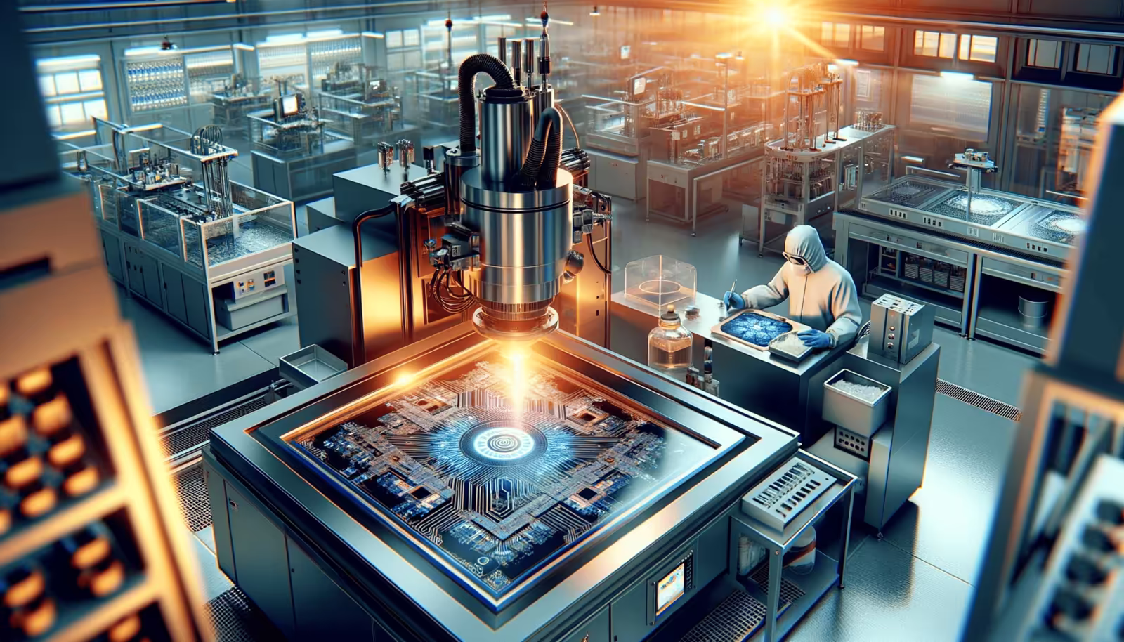
Photoresist removal is a critical step in the semiconductor device production process. It's essential to understand the importance of this process and the technologies involved, such as UV-Ozone and plasma ashing.
Photoresists are temporary masks used for structuring steps in semiconductor production. After these steps, the resist must be removed efficiently and completely without leaving any residue.
In semiconductor manufacturing, lithography is a key process where patterns are transferred onto a substrate using a light-sensitive material called photoresist. After the patterning is complete, it's crucial to remove the photoresist to proceed with subsequent manufacturing steps like etching or ion implantation. Inadequate removal can lead to defects or performance issues in the final semiconductor device.
Photoresist removal is a crucial yet delicate process in semiconductor manufacturing, balancing the need for efficiency, high throughput, and minimal damage to sensitive materials. The choice between UV-Ozone and plasma ashing techniques depends on the specific requirements of the semiconductor device and the materials involved.
Plasma Ashing
Plasma ashing uses a combination of ions and radicals for photoresist removal. RIE, in particular, is effective due to the combination of physical sputtering by ions and chemical reactions by radicals. However, it has drawbacks like the potential for plasma damage due to reactive ions, which can physically damage the substrate.
UV-Ozone
UV-Ozone Ashing is a method that involves the use of oxygen radicals generated by UV light and ozone for ashing the photoresist. It's a dry process, meaning it doesn't require solvents. UV-Ozone ashing is particularly effective for photoresist removal on damage-sensitive layers due to its gentle nature.
What Industries Need Photoresist Removal?
Photoresist removal is a critical process in various industries that rely on precise microfabrication and microstructuring techniques.
Semiconductor Industry
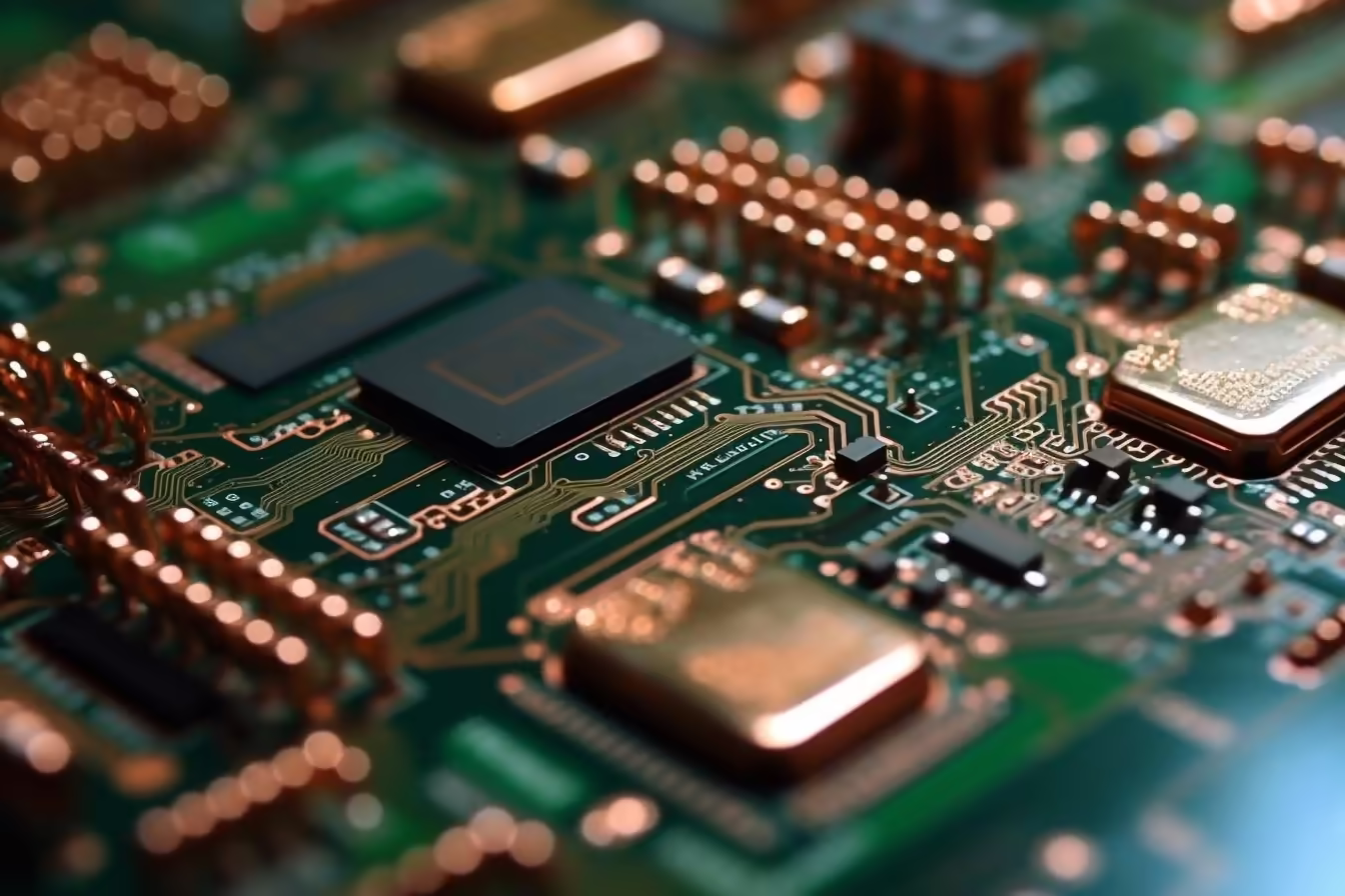
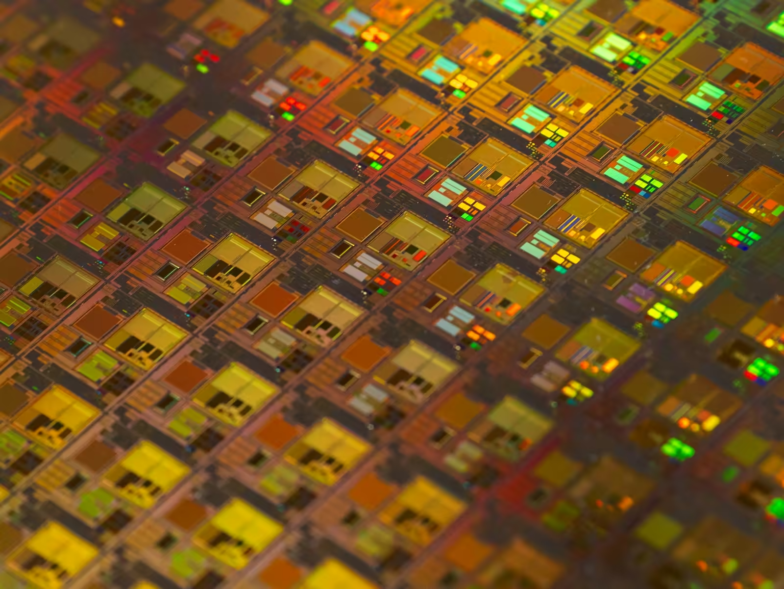
In the production of integrated circuits and microchips, photoresist is used to create intricate patterns on silicon wafers. After these patterns are etched onto the wafer, the photoresist must be completely removed to avoid interference with subsequent manufacturing steps and to ensure the functionality of the chips.
Techniques like flip-chip bonding and wafer-level packaging also require photoresist for patterning and therefore necessitate effective removal methods.
Microelectronics
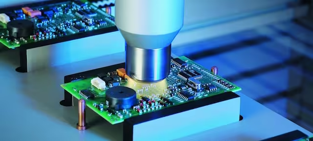
The photoresist is used to pattern the conductive traces on PCBs (Printed Circuit Board). After etching these traces, the photoresist is removed to expose the final circuit design. MEMS (Micro-Electro-Mechanical Systems) which combine mechanical and electrical components at a microscale, use photoresist in their fabrication process, requiring precise removal techniques.
Photonics and Optoelectronics
Photoresist is used in the manufacturing of various optical components like lenses, waveguides, and gratings. The removal of photoresist in these processes is crucial to achieve the desired optical properties.
Solar Panel Manufacturing
Photoresist is used to create patterns for anti-reflective coatings or conductive paths on solar cells. Proper removal is essential to maximize the efficiency and performance of the solar panels.
Biotechnology and Medical Devices
In the fabrication of microfluidic chips, which are used for various biological and chemical analyses, photoresist patterning and subsequent removal are key steps. Some biosensors and medical implants require microscale patterning, where photoresist plays a role.
Research and Development
In academic and industrial research, photoresist is often used for prototyping micro and nanoscale devices, necessitating removal processes in the development phase.
Final Thoughts
The removal of photoresist is a pivotal process not only in semiconductor manufacturing but across a broad spectrum of industries that rely on precision microfabrication. The choice of removal technique, be it plasma ashing or UV-Ozone ashing, hinges on the specific requirements of the project, including the type of photoresist used, the sensitivity of the materials involved, and the desired outcome of the end product.
From enhancing the performance of integrated circuits in the semiconductor industry to the intricate patterning required in photonics, microelectronics, solar panel manufacturing, and biotechnology, effective photoresist removal is essential.
Reaching out to a specialized company like SCI Plasma can be invaluable. As experts in the technology of plasma, we bring a wealth of knowledge in plasma cleaning and surface treatment systems. Working with us offers an opportunity to gain insights and support specifically designed for your technological challenges. Contact us today.