The need for reliable and efficient manufacturing processes has never been greater in the electronics industry. One of the unsung heroes in meeting these demands is plasma treatment technology. It offers numerous benefits that not only optimize the manufacturing process but also contribute to the long-term reliability and performance of electronic components.
This article delves into the various advantages of plasma cleaning in the electronics industry, exploring how this innovative technology serves as a pillar of modern electronics manufacturing.
What is Plasma Cleaning and Plasma Treatment?
Plasma is a flexible and adaptable technology that can work on a variety of materials, making it highly desirable for numerous applications, particularly in the detail-focused electronics industry.
What Is Plasma?
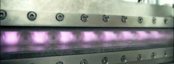
Before diving into plasma cleaning, it's essential to understand what plasma is. Plasma is the fourth state of matter, alongside solids, liquids, and gases. It consists of a mixture of electrons, ions, and molecules that have been subjected to high-energy conditions. This is usually done through electrical, radiofrequency, or microwave energy. This high-energy environment results in an ionization of the gas molecules.
The Science Behind Plasma Cleaning
Plasma cleaning uses this highly reactive environment to interact with surface contaminants or contagions. When plasma comes into contact with a material surface, the plasma's charged particles collide with the object at the atomic level. These interactions can result in breaking the chemical bonds of surface contaminants or contagions, effectively cleaning, sterilizing, or modifying the surface at an infinitesimal level.
The process often employs gases like argon, oxygen, hydrogen, or nitrogen, depending on the type of cleaning required. In some applications, a combination of gases is used to achieve specific cleaning effects.
What Is Plasma Treatment?
Plasma treatment is a surface modification process that utilizes plasma to alter the physical, chemical, or mechanical properties of the surface of an object. Plasma can effectively clean, sterilize, and enhance the adhesion or wettability of a wide range of objects. Plasma treatment offers a powerful solution for improving material properties without affecting the bulk of the material, making it widely applicable in industries such as electronics and others.
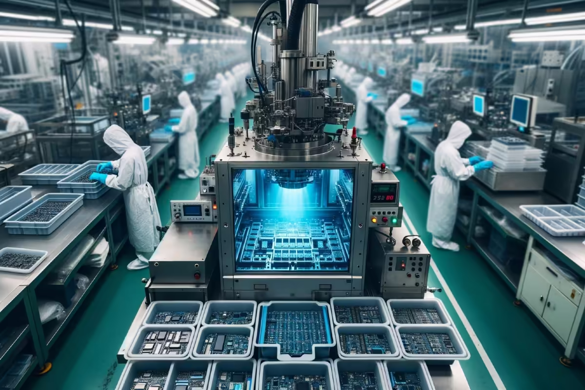
How Is Plasma Cleaning Used in the Electronics Industry?
Plasma cleaning has become an indispensable tool in the electronics manufacturing process. It ensures not only the functionality but also the long-term reliability of electronic devices, making it a cornerstone technology in the industry.
Here, we highlight some of the main uses of plasma cleaning technology in the electronics industry:
Ultra-Clean
In the electronics industry, there is a focus on miniaturization while maintaining functionality. This makes cleanliness and precision paramount in the manufacturing processes. Microscopic levels of contamination can result in defects, malfunctions, or outright failure of electronic devices. This means that traditional cleaning methods such as solvents or manual wiping are insufficient.
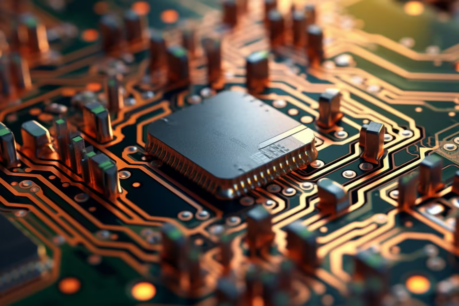
Cleaning Printed Circuit Boards (PCBs)
One of the most common applications of plasma cleaning in electronics is the cleaning of printed circuit boards (PCBs). After the soldering process, residues such as solder flux and rosin often remain on the board. These residues can lead to electrical shorts, reduced insulation resistance, and overall compromised performance. Plasma cleaning effectively removes these contaminants, improving both the reliability and longevity of the PCBs.
Component Preparation
Prior to assembly, electronic components like semiconductor wafers, connectors, and various IC (integrated circuit) packages must be impeccably clean to ensure optimal electrical contact and adhesive bonds. Plasma cleaning removes organic contaminants, thus enhancing surface wettability and ensuring that subsequent processes, like wire bonding or epoxy application, are more reliable.
Wire Bonding
In essence, wire bonding is a method used to connect semiconductor devices to their packages. Before the wire bonding process, the surfaces involved must be extremely clean to form a strong, reliable bond. Plasma cleaning effectively removes any oxidation and contaminants that could interfere with this bonding, thereby significantly improving bond integrity and device performance.
Package Molding
Electronic components often have to be sealed in packages to protect them from environmental factors such as moisture, dust, and temperature variations. However, organic contaminants on the surface can compromise the seal. Plasma cleaning is used to remove these contaminants, ensuring a more robust and long-lasting package seal.
Conformal Coating
Before performing the conformal coating process on electronic components to protect them from environmental factors, it is crucial that the surface is free of any contaminants that could interfere with the adhesion of the coating. Plasma cleaning serves to prepare the surface, making it more receptive to the conformal coating, which in turn enhances its effectiveness and longevity.
What Are the Advantages of Plasma Cleaning in the Electronics Industry?
The advantages of plasma cleaning in the electronics industry are numerous, ranging from operational efficiency and cost-saving to environmental sustainability and product reliability. These benefits make plasma cleaning a cornerstone technology in modern electronics manufacturing.
1. Efficiency
One of the most compelling advantages of plasma cleaning is its efficiency. Unlike traditional cleaning methods, which can be time-consuming and labor-intensive, plasma cleaning often takes only a few minutes to treat surfaces. This speed is especially beneficial in high-throughput manufacturing processes where time is of the essence.
2. Eco-Friendly
Plasma cleaning eliminates the need for harsh chemical solvents, which can be hazardous to both the environment and the workers who handle them. This results in a cleaning process that is safer and more ecologically responsible. The absence of chemical waste also means that disposal costs and regulatory compliance burdens are reduced, making it a sustainable choice for the long term.
3. Uniformity of Treatment
Plasma cleaning provides unparalleled uniformity, an essential factor when dealing with complex geometries or microscopic features commonly found in electronic components. The plasma can penetrate fine features, ensuring that all surfaces, including hidden or hard-to-reach areas, are uniformly cleaned. This level of uniformity is difficult to achieve with liquid solvents or mechanical cleaning methods.
4. Cost-Effective
The initial setup for a plasma cleaning system might involve some investment, the long-term benefits make it a cost-effective solution. Savings come from reduced consumption of cleaning agents, lower disposal costs, and fewer man-hours spent on the cleaning process. Moreover, by reducing the rate of product failure due to contamination, plasma cleaning also contributes to cost-saving.
5. Improved Adhesion
Plasma cleaning offers more than just contaminant removal; it also alters the surface of the substrate. This change in properties enhances the adhesion of materials in subsequent processes, such as bonding or coating. Better adhesion leads to more reliable products, whether that means stronger wire bonds in semiconductor devices or more durable conformal coatings on PCBs, as we discussed above.
Final Thoughts
Plasma cleaning has emerged as an indispensable tool in the electronics manufacturing process where efficiency and reliability are at the core of success. Its myriad advantages, ranging from operational efficiency to environmental sustainability, make it a cornerstone technology for producing electronic components that meet the high standards of modern life.
For those in the industry looking to harness the potential of plasma cleaning and plasma treatment technologies, SCI Automation stands as an industry leader. Our team offers state-of-the-art plasma treatment solutions tailored to specific manufacturing needs. With our expertise and commitment to innovation, SCI Automation is well-positioned to help you navigate the complexities of modern electronics manufacturing, ensuring that your products not only meet but exceed quality and reliability standards. Reach out today.