
In semiconductor manufacturing, plasma cleaning uses ionized gases to eliminate residues before lithography and bonding, increasing yield and reliability.
How Plasma Cleaning Works in Semiconductors
The typical semiconductor plasma cleaning setup involves:
- Argon Plasma Cleaning – Used to strip away organic residues from lead frames, wafers, and pads.
- Surface Activation – Plasma excites the surface, increasing surface energy for optimal adhesion.
Process Control – The recipe (gas flow, power, pressure, duration) is tightly controlled to avoid damaging delicate parts.
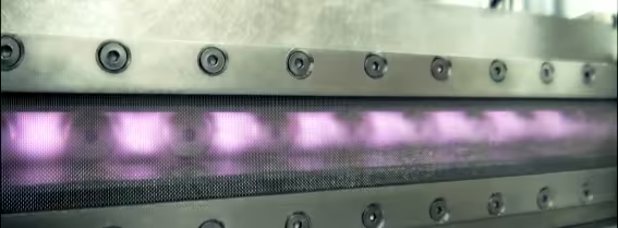
In sensitive applications, direct plasma configurations are used. The electrode is positioned above the part to prevent direct RF contact—ideal for parts susceptible to damage.
Leaky chambers or poorly tuned recipes can lead to issues like oxidation. For example, if oxygen leaks in from outside, it can leave oxidation marks on wire bond pads.
Benefits of Plasma Cleaning in Semiconductor Processes
Sub-micron Contaminant Removal
- Removes carbon-based residues invisible to visual inspection
Prepares surfaces for consistent wire bonding and mould adhesion
Oxide Layer Removal
- Restores exposed bare metal
Especially effective with hydrogen plasma for oxide-sensitive surfaces
No Wet Chemicals
- Avoids ionic contamination and disposal risks
Clean, dry, and environmentally stable
Protects Sensitive Substrates
Tunable process parameters prevent plasma damage
Direct plasma mode available for high-precision components
Applications in Semiconductor Manufacturing

Wire Bonding Preparation
- Ensures bond pads are free of oxides and organic contaminants
Prevents NSOP (Non-Stick-On-Pad) failures
Die Attach and Underfill
- Improves adhesion for epoxies and adhesives
Reduces voiding and delamination
Lead Frame Cleaning
Enhances bondability and plating consistency
Flip Chip Assembly
Ensures bump contact reliability by cleaning interconnects
Wafer-Level Packaging (WLP)
Prepares die surfaces for redistribution layer (RDL) deposition
Types of Plasma Systems for Semiconductor Lines
Batch Plasma Systems
- Common in lead frame cleaning or high-mix, low-volume lines
Controlled, uniform exposure
Inline Plasma Systems
- Integrated into bonding or assembly lines
Enables high-throughput and traceability
Direct Plasma
Minimises direct RF contact
Hydrogen Plasma
- Specially used for oxide removal
- Restores metal surfaces like copper or aluminium
Plasma cleaning is not just another prep step—it's foundational to long-term device reliability. With the right system and tuning, it can protect sensitive parts, reduce rejects, and improve final yield.
If your plasma process is damaging your product, it may be time to review your setup. Chamber leaks and recipe errors are often the culprits.
Need to troubleshoot your process or evaluate a better fit for your production line? Talk to a plasma expert who can match the right tool to your application.
FAQs
Why is plasma cleaning preferred in wire bonding?
It removes invisible residues and oxides, allowing for better intermetallic bonds and reduced NSOP defects.
Can plasma damage my device?
Only if poorly configured. With the right parameters or direct plasma setup, damage can be avoided.
What gas is used in semiconductor plasma cleaning?
Argon is common for cleaning. Hydrogen is used for oxide removal. Oxygen can cause unwanted oxidation if not controlled.
Is plasma cleaning better than wet cleaning for semiconductors?
Yes. Plasma is residue-free, dry, and controllable—critical for microelectronics.
What issues can occur in a faulty plasma process?
Oxidation marks, incomplete cleaning, or substrate damage—typically from oxygen leaks or incorrect recipes.