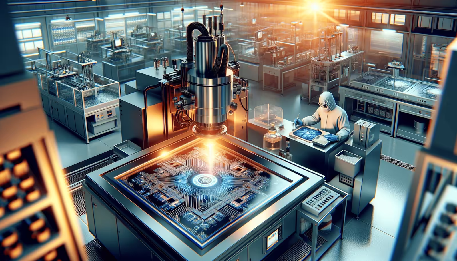
Dry etching is a highly precise method of removing material from the surface of an object by bombarding it with an ionized gas called plasma. It meticulously eliminates the thinnest of layers, making it ideal for applications requiring extreme accuracy. The plasma comprises various chemicals that react with the surface, carving thin walls and lines into the material.
Dry etching is frequently employed in semiconductor fabrication, a crucial component in electronic devices. It operates distinctly from wet etching, which relies on liquid chemicals to remove material. Dry etching offers exceptional precision, ensuring the process is confined to specific regions and depths on the object, without unintentional spreading.
In this article, we will delve into the inner workings of plasma dry etching, providing a step-by-step explanation of the process, discussing the three main types of plasma dry etching, and guiding you in determining if dry etching is the most suitable choice for your specific needs.
What Is Plasma Dry Etching?
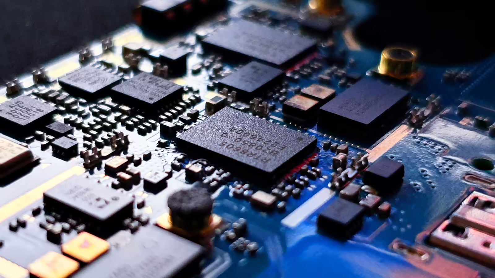
Dry etching is a vital process employed in the fabrication of semiconductors and other materials found in electronic devices. It enables the creation of minuscule holes or shapes in these materials, paving the way for the formation of contact lanes that connect different parts of a semiconductor, or via lanes that establish paths between distinct conductive layers. Moreover, dry etching can be utilized to shape the semiconductor in specific ways, such as forming vertical sides.
Dry etching offers notable advantages, as it can be applied to materials resistant to traditional wet etching methods. Furthermore, it is a more cost-effective solution that necessitates less equipment compared to other manufacturing techniques. Consequently, dry etching has become a popular choice for producing extremely small electronic devices, including various semiconductors and printed circuit boards.
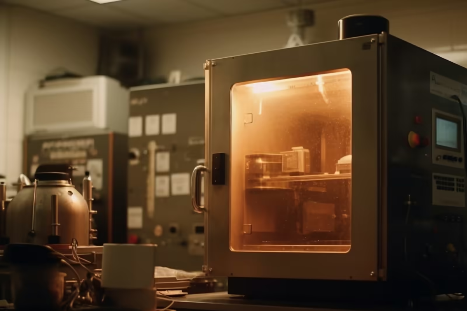
A Step-by-Step on How Dry Etching Works
Step 1
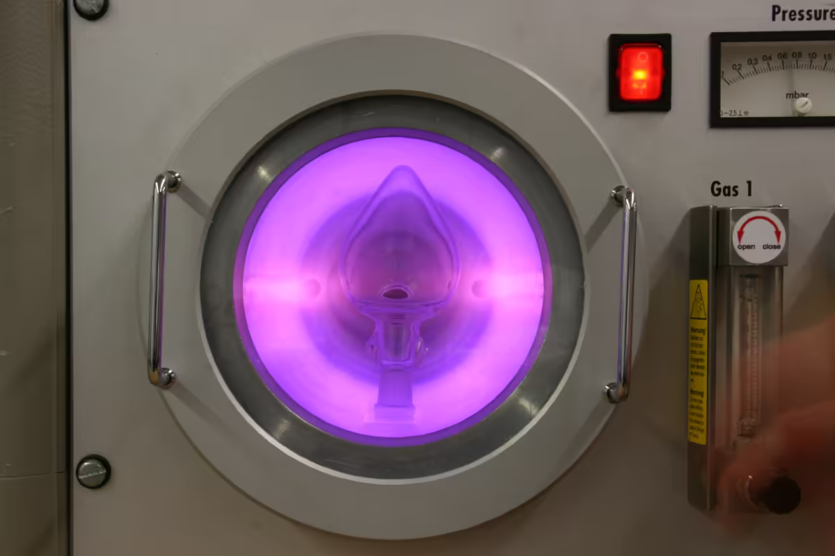
A wafer or product is placed inside a vacuum plasma chamber on an electrode connected to an RF source.
Step 2
Plasma is generated in the chamber, which contains free electrons and positively charged ions.
Step 3
The ions present in the plasma are accelerated towards the product inducing reactions with the product surface vaporizing parts of it. This effectively removes layers of the products.
3 Types of Plasma Dry Etching
1. Reactive Ion Etching (RIE)
RIE is a chemically driven process that involves the use of reactive species (ions, radicals) generated by a plasma to etch the surface of the target material. RIE is can be used to create anisotropic etching patterns, meaning it can etch preferentially in a specific direction, resulting in a high degree of control and vertical sidewalls.
The process is carried out in a vacuum plasma chamber, where a gas mixture is ionized using a radio-frequency (RF) source. The reactive ions generated in the plasma chemically react with the target material, forming volatile by-products that can be removed.
RIE is commonly used for the fabrication of micro-electromechanical systems (MEMS), integrated circuits (ICs), and other microstructures requiring high precision and sharp features.
2. Sputter Etching
Sputter etching is a physical process that involves bombarding the target material with high-energy ions or particles, causing the ejection of surface atoms. Sputter etching is less directional and more isotropic than RIE, meaning that it etches uniformly in all directions.
The process is typically carried out in a vacuum chamber, where a plasma is generated using a separate target (sputtering source) and accelerated toward the substrate to be etched.
Sputter etching is often used for thin-film deposition, surface cleaning, or modification, and etching materials that are resistant to chemical etching.
3. Vapor Phase Etching
Vapor Phase Etching is a dry etching technique that involves the use of reactive gas-phase species to selectively remove material from a substrate without direct contact. Unlike other dry etching techniques like Reactive Ion Etching (RIE) and Sputter Etching, Vapor Phase Etching is primarily a chemical process that does not rely on ion bombardment or plasma generation.
In Vapor Phase Etching, the reactive gas is introduced into a reaction chamber containing the substrate to be etched. The gas molecules react chemically with the surface material, forming volatile reaction products that can be easily removed by a vacuum system. The etching process can be highly selective, depending on the choice of reactive gas and the material to be etched.
One well-known example of Vapor Phase Etching is the use of anhydrous hydrogen fluoride (HF) gas for etching silicon dioxide (SiO2) selectively while leaving silicon (Si) or other materials intact. This selectivity is particularly useful in the semiconductor industry for the fabrication of microelectronic devices.
Overall, Vapor Phase Etching is a less common dry etching technique compared to RIE or Sputter Etching, but it can be advantageous in specific applications where a gentle, chemically driven, and highly selective etching process is desired.
Is Dry Etching Right For You?
Essentially, plasma dry etching is an essential manufacturing technique in the electronics industry, particularly for semiconductors and printed circuit boards. This process offers several advantages over traditional wet etching methods, including increased precision and cost-effectiveness.
With three primary types of plasma dry etching—Reactive Ion Etching (RIE), Sputter Etching, and Vapor Phase Etching—there are multiple options for achieving the desired etching results. By understanding the step-by-step process of dry etching and its various types, engineers and manufacturers can select the most appropriate method for their specific needs, ensuring optimal results in the creation of intricate electronic devices.
As the choice of the most suitable plasma dry etching technique depends on factors such as the material being etched, the desired outcome, and specific project requirements, it is highly recommended to consult with experts in the field. By engaging with experienced professionals, such as SCI Plasma, you can gain valuable insights into the various etching processes and their intricacies.
These experts can help you identify the optimal technique tailored to your needs, ultimately enhancing the efficiency and success of your project. Partnering with knowledgeable specialists in the plasma dry etching domain will ensure that you make well-informed decisions and achieve the best results for your electronic devices.