

Plasma Cleaning for Semiconductor Manufacturing
Sub-micron contamination on lead frames, dies and bond pads is invisible to the eye and lethal to yield. Vacuum plasma cleaning removes it before it becomes a bond failure.
In semiconductor packaging, the surface you can't see is the one that decides whether a device works. Oxide layers a few nanometres thick, organic residues left over from prior process steps, and sub-micron particulates don't show up on a visual inspection station, but they sit directly between a wire and a bond pad, or between a die and a mould compound. When that boundary is contaminated, the bond that forms across it is weaker than the process was designed to deliver — and the failure doesn't show up as a rejected part today, it shows up as an intermittent field failure months later.
The problem: contamination hides upstream of every packaging step
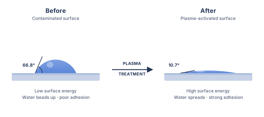
Wire bonding, die attach, underfill and transfer molding are all adhesion processes, and adhesion is a surface phenomenon. Oxidation blocks intermetallic formation between a gold or copper wire and an aluminium or copper pad, preventing the metallurgical bond from forming at all. Organic residues — flux, mould-release agents, handling oils — sit as a physical barrier between an epoxy and the substrate it's meant to wet. Both conditions show up as a measurable drop in surface energy, visible as a high water contact angle: untreated lead frames and dies commonly test above 60°, sometimes closer to 67°. A high contact angle means poor wettability, and poor wettability means the adhesive, the wire bond, or the mould compound is fighting the surface instead of keying into it.
The downstream symptoms are familiar to anyone running a packaging line: NSOP (non-stick-on-pad) failures during wire bonding, low pull- and shear-test values that pass inspection but sit close to the reject threshold, voiding and delamination under underfill or mould compound, and early-life field failures that never show a root cause in final test. None of these are fixed by adjusting the bonder or the moulding press — the machines are working the surface they're given, and that surface was already compromised before the part reached the tool.
Where vacuum plasma cleaning fits
Vacuum plasma cleaning treats the surface directly, at the point in the process where it matters: immediately before the adhesion step, not after a failure is caught downstream. Inside a vacuum chamber, a process gas — typically argon for organic residue removal, hydrogen for oxide-sensitive metal surfaces, or oxygen for photoresist ashing and descum — is energised into a plasma. The ionised species in that plasma physically and chemically strip sub-micron organic contamination and thin oxide layers from the surface, while simultaneously raising its surface energy through activation. The process is entirely dry: there's no wet-chemical residue to rinse, no ionic contamination to manage, and no disposal stream to permit.
The effect is not subtle. A typical lead frame or die surface with a water contact angle around 67° drops to roughly 11° after an argon plasma cycle — a shift from a surface that resists wetting to one that actively promotes it. That change is what makes the difference between a wire bond that forms a reliable intermetallic and one that lifts under a pull test.
Process parameters — gas selection, RF power, chamber pressure, cycle duration — are tuned per part, and for RF-sensitive components a direct plasma configuration (electrode positioned above the part rather than in direct contact) keeps the treatment gentle enough for delicate dies and thin lead frames. Left untuned, or with a leaky chamber letting in ambient oxygen, the same process can go the other way and leave oxidation marks on the pads it was meant to clean — which is why recipe control and chamber integrity matter as much as the plasma step itself.
Where it sits in the packaging flow
Plasma cleaning is a pre-treatment step, not a rework step, and it integrates ahead of the processes where surface condition determines outcome:
- Wire bonding preparation — strips oxides and organics from bond pads and lead frames, eliminating NSOP failures and lifting pull/shear strength.
- Die attach and underfill — improves epoxy and adhesive wetting, reducing voiding and delamination under the die.
- Transfer molding — activates lead frame and substrate surfaces ahead of the mould compound, reducing mould-related yield loss.
- Lead frame cleaning — enhances bondability and plating consistency across a full magazine, not just the parts an inspector happened to sample.
- Flip chip and wafer-level packaging — cleans bump interconnects and prepares die surfaces ahead of redistribution-layer deposition.
- Plasma descum — removes residual photoresist left in trenches and vias after development, ahead of etch, so subsequent patterning is not thrown off by nanometre-scale residue.
Matching the system to the line
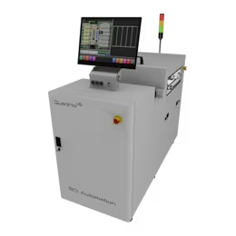
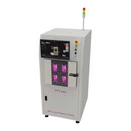
The right plasma system depends on part geometry and throughput, not just chamber size. Quadrio Alpha is a magazine-fed, semi-automatic system purpose-built for lead frame processing: each frame is pulled from its magazine, plasma-treated, and returned to the same magazine, with up to five magazines processed concurrently and full per-frame traceability available for MES integration — the configuration most semiconductor packaging houses standardise on for lead frame prep ahead of wire bonding and transfer molding. Titan is the magazine-fed batch alternative for lead frames, holding up to six magazines in fixed positions so every frame is treated evenly regardless of magazine size; because it cycles frames through the chamber in place rather than by automated pick-and-place, it is the gentler choice for fragile frames or ones already carrying formed wire bonds that must not be disturbed.
Verifying the result
A plasma step that isn't measured is a plasma step you're trusting on faith. Contact-angle measurement before and after treatment is the fastest verification available on the line — it directly tracks the wettability that drives bond quality, and a drift back toward the untreated baseline is an early warning of a chamber or recipe problem before it shows up as a bonding defect. Downstream, correlating plasma cycle data against wire-bond pull/shear-test results and NSOP rate closes the loop between the surface-prep step and the metric that actually matters: yield.
Recommended systems
Related applications
Related articles

What is the Plasma Cleaning Process in the Semiconductor Industry?
In semiconductor manufacturing, plasma cleaning uses ionized gases to eliminate residues before lithography and bonding, increasing yield and reliability.
Why Your Wire Bonding Is Failing and How to Fix It with Plasma Cleaning
Wire bonding failures don't happen by accident, and blaming machines or operators misses the real problem.

The Use Of Plasma In The Semiconductor Industry
In the semiconductor industry, plasma processes are critical for manufacturing high-quality electronic devices with precision and efficiency
Frequently asked questions
What does plasma cleaning actually remove from semiconductor surfaces?
Sub-micron organic residues (flux, mould-release agents, handling oils) and thin oxide layers on lead frames, dies and bond pads — contamination that's invisible to a visual inspection station but sits directly in the bond line.
How much does surface contact angle actually change after treatment?
Typical lead frame and die surfaces test around 67° before treatment and drop to roughly 11° after an argon plasma cycle, a shift from a wetting-resistant surface to a wetting-active one.
Will plasma cleaning damage sensitive dies or thin lead frames?
Only if the recipe or chamber is misconfigured. Tunable gas, power, pressure and duration parameters, plus a direct plasma configuration for RF-sensitive parts, keep the process within the tolerance of delicate components.
Should we run batch or inline plasma cleaning?
For lead-frame packaging it is usually batch: a magazine-fed system treats each frame in its own magazine, which is gentler than carrier handling and keeps per-frame traceability. Quadrio Alpha (up to five magazines) is the configuration most packaging houses standardise on ahead of wire bonding and transfer molding, and Titan is the magazine-fed batch alternative, holding up to six magazines and handling fragile or already-wire-bonded frames gently. Inline systems earn their place on high-volume module and PCB lines, not on lead-frame prep.
How do we verify the plasma step is actually working, not just running?
Track water contact angle before and after treatment as a direct wettability check, and correlate plasma cycle data against downstream wire-bond pull/shear-test results and NSOP rate so a drifting chamber shows up before it becomes a yield event.